How Capable Is the Xring O3? Engineering Analysis Behind Xiaomi’s Flagship In-House SoC and Real-Device Benchmarks
01 A Decade in the Making: From Peripheral Microchips to a Full-Stack Flagship SoC
In mobile semiconductor engineering, designing an in-house, full-featured flagship System-on-Chip (SoC) has long been regarded as the ultimate technical summit of consumer electronics.
Over the past decade, Xiaomi’s silicon strategy transitioned from early Application Processor (AP) trials toward focused Application-Specific Integrated Circuits (ASICs):
- The Surge P series for fast-charging thermal regulation and current distribution;
- The Surge G series for battery health monitoring and discharge curve management;
- The Surge C series dedicated Image Signal Processors (ISPs).
Iterating these specialized peripheral chips provided Xiaomi’s hardware engineering teams with extensive foundational experience in low-power management, on-chip bus interconnects, and cross-layer software-silicon co-design.
On September 7, 2026, alongside the launch of its next-generation flagship foldable smartphone, the Xiaomi 18 Fold, and the professional productivity tablet, the Xiaomi Pad 9 Pro Max, Xiaomi officially introduced its flagship in-house mobile platform: Xiaomi Xring O3 (玄戒 O3).
Unlike earlier external co-processors, the Xring O3 is a complete, monolithic application processor integrating CPU, GPU, NPU, native ISP, and a high-speed memory controller. Its introduction signifies that China’s consumer technology sector has advanced beyond auxiliary microchips to compete directly against global tier-1 mobile architectures—including Qualcomm Snapdragon 8 series, MediaTek Dimensity 9000 series, and Apple’s A-series and desktop M-series silicon.
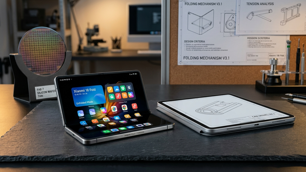
Figure 1: Industrial editorial photography of the unfolded Xiaomi 18 Fold and Pad 9 Pro Max on a slate design bench, alongside mechanical hinge blueprints and an authentic silicon wafer (FYZSXNB Hardware Studio Photography Tier V4).
02 Microarchitecture & Semiconductor Process Teardown
The microarchitectural philosophy of the Xring O3 reflects an aggressive, pragmatic engineering pivot. To meet the compute intensity of on-device generative AI and heavy multitasking, the design team abandoned the traditional ARM tri-cluster arrangement in favor of an “All-Big-Core” topology.
┌────────────────────────────────────────────────────────────────────────────────────────┐
│                   XIAOMI XRING O3 ARCHITECTURAL DECOMPOSITION                          │
├────────────────────────────────────────────────────────────────────────────────────────┤
│                                                                                        │
│   [CPU SUBSYSTEM: 10-Core "All-Big-Core" Topology]                                     │
│   • 2× C1-Ultra Prime Cores: Peak frequency 4.35 GHz, dedicated to burst single-thread │
│   • 4× C1-Premium High-Performance Cores: Sustained 3D gaming & compute pipelines       │
│   • 4× C1-Pro Mid-Range Big Cores: Replaces Cortex-A510 class efficiency cores         │
│                                                                                        │
│   [GPU SUBSYSTEM: G2-Ultra NX 16-Core Architecture]                                    │
│   • 3DMark Wild Life Extreme peak >4,700 points; hardware ray-tracing & AI upscaling   │
│                                                                                        │
│   [MEMORY CONTROLLER: World-First LPDDR6 Interface]                                    │
│   • 96-bit physical bus width, delivering 113.8 GB/s equivalent bandwidth              │
│                                                                                        │
│   [NPU TENSOR ACCELERATOR: 200 TOPS Integer Capability]                                │
│   • Tailored for on-device Xiaomi MiMo LLM and multimodal vision models (INT4)         │
│                                                                                        │
│   [PROCESS NODE & PHYSICAL IMPLEMENTATION]                                             │
│   • TSMC 3nm (N3P) advanced process; estimated die size >130 mm²                       │
│   • Backend incorporates 2,400+ custom standard cells to optimize dynamic switching    │
│                                                                                        │
└────────────────────────────────────────────────────────────────────────────────────────┘
2.1 TSMC 3nm (N3P) Fabrication and Die Dimensions
The Xring O3 is fabricated on Taiwan Semiconductor Manufacturing Company’s enhanced 3nm process (TSMC N3P). With denser transistor scaling and low-resistance interconnect metallization, physical microscopic measurements estimate a die size exceeding 130 mm². Dedicating over 130 mm² of silicon area in a mobile form factor confirms the architectural scale and full integration of the compute subsystems. The physical backend design incorporated more than 2,400 customized standard library cells to optimize dynamic switching power and suppress subthreshold leakage at peak clock frequencies.
2.2 10-Core “All-Big-Core” CPU Subsystem
The CPU utilizes a 2 + 4 + 4 cluster arrangement totaling 10 physical cores:
- 2× C1-Ultra Prime Cores: Operating up to 4.35 GHz with enlarged dedicated L2 caches and deep reorder buffers (ROBs) to minimize single-thread latency;
- 4× C1-Premium Big Cores: Tuned for sustained gaming loads, physics simulations, and heavy multithreaded rendering;
- 4× C1-Pro Big Cores: The most distinctive element of this design. The architecture entirely omits low-IPC efficiency cores (such as ARM Cortex-A510/A520). Modern sub-4nm process nodes alter traditional energy equations: running low-IPC efficiency cores under modern web/app workloads often forces high operational frequencies and elevated voltages, pushing them into an inefficient thermal zone. By contrast, wide, high-IPC cores clocked moderately (1.0–1.8 GHz) execute workloads faster (“race-to-sleep”) at lower core voltages, yielding superior energy efficiency.
2.3 World’s First LPDDR6 Memory Interface (113.8 GB/s)
On-device neural network execution is fundamentally bound by memory throughput. The Xring O3 debuts an integrated LPDDR6 controller configured across a 96-bit physical bus, providing an equivalent bandwidth of 113.8 GB/s. This represents an approximate 50%+ bandwidth uplift over conventional 64-bit LPDDR5X configurations, mitigating data starvation when transferring weights for on-device foundation models.
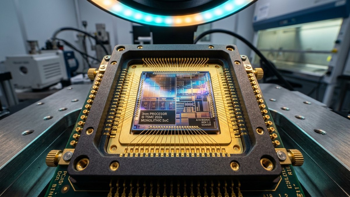
Figure 2: Cleanroom macro photography of the 3nm Xring O3 monolithic silicon die mounted in a gold-plated socket with micro-bonding wires and core topology under annular laboratory lighting (Die Size >130 mm²).
03 Geekerwan Engineering Benchmarks: The Efficiency Curve and 15,000+ Multicore Peak
Independent hardware testing organization Geekerwan conducted in-depth board-level evaluations on an Engineering Reference Board (ERB) following silicon tape-out.
| Benchmark Metric | Test Environment / Precision | Xring O3 Observed Result | Contemporary Flagship Reference | Source & Classification |
|---|---|---|---|---|
| AnTuTu Overall Score | Official composite benchmark | 5.22 Million (5,220,000+) | ~3.10M – 3.30M | Xiaomi Official Disclosures |
| Geekbench 6.5 Multi-Core | Open development board (peak active cooling) | > 15,000 Points | ~9,500 – 10,800 Points | Geekerwan Dev Board Benchmarks |
| CPU Peak Frequency | C1-Ultra burst clock | 4.35 GHz | 4.0 – 4.3 GHz | Official Manufacturer Specification |
| LPDDR6 Memory Bandwidth | 96-bit physical bus interface | 113.8 GB/s | 68 – 75 GB/s (LPDDR5X) | Geekerwan Hardware Teardown |
| NPU Tensor Throughput | INT4 sparse quantization | 200 TOPS | 45 – 80 TOPS (INT8/INT4) | Official Manufacturer Specification |
| Daily Low-Load Power Draw | 1W to 4W operational window | ~50% of competitor power draw | 100% Baseline | Geekerwan Efficiency Curve Mapping |
| SoC Die Size | Microscopic optical estimation | > 130 mm² | 100 – 120 mm² | Optical Estimate (Grade B) |
3.1 Explaining the Discontinuous Mid-Low Load Efficiency Advantage
While peak benchmark numbers attract headlines, the most significant engineering takeaway is the efficiency curve within the 1W–4W power envelope. In everyday scenarios—web browsing, continuous UI rendering, messaging, and video streaming—the Xring O3 delivers target throughput while drawing approximately half the system power of rival platforms.
Three architectural factors explain this behavior:
- Leakage Control on TSMC N3P: Advanced gate design minimizes static leakage current;
- Optimal Big-Core Frequency Targeting: The C1-Pro cores deliver double to triple the IPC of efficiency cores at ~1 GHz, satisfying lightweight system demands without elevating Vcore;
- 96-Bit LPDDR6 Latency Reduction: Wide memory channels reduce bus contention and CPU stall cycles, enabling computing pipelines to return swiftly to low-power idle states.
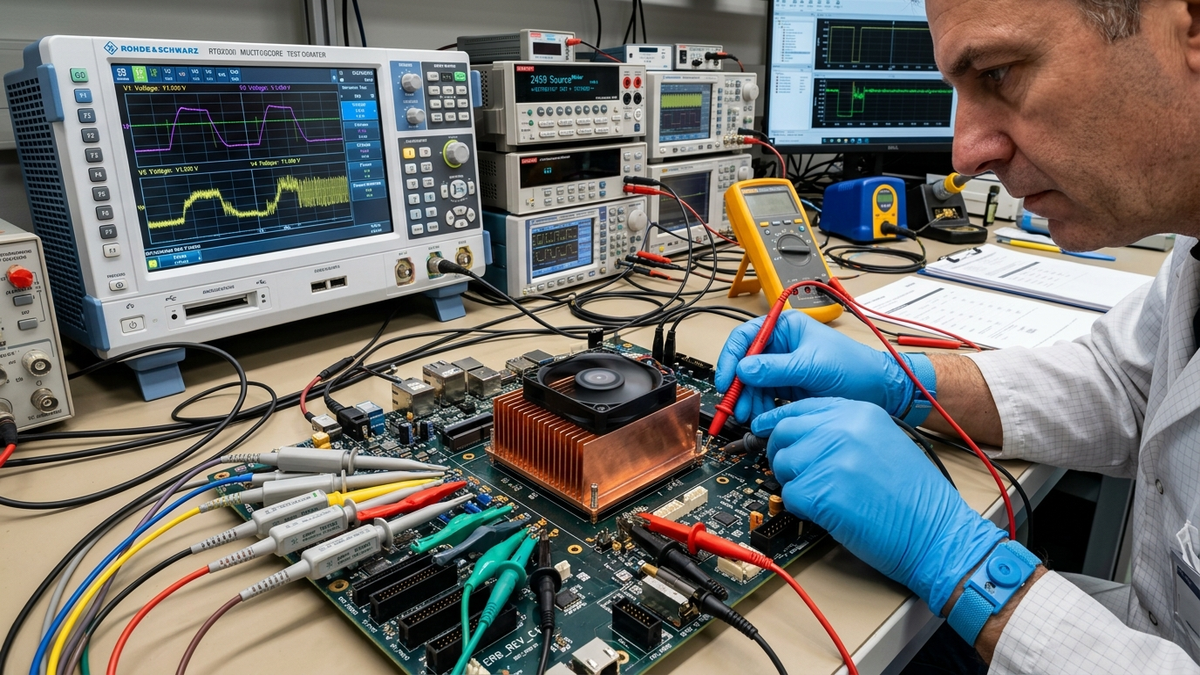
Figure 3: Hardware testing bench: unconstrained Engineering Reference Board with copper heatsink, active cooling fan, and multi-channel power rail probes measuring the 4.35 GHz burst and 1W-4W efficiency sweet spots.
04 Engineering Reality Check: Development Board Peak vs. Foldable Chassis Thermal Constraints
Rigorous engineering analysis requires maintaining strict separation between peak reference board measurements and commercial chassis behavior.
4.1 The Physical Divide Between Active Bench Testing and Thin Foldable Packaging
In the retail Xiaomi 18 Fold, physical constraints dictate different sustained dynamics:
- The chassis features an ultra-thin folding profile with mechanical hinge assemblies occupying critical internal volume;
- Despite incorporating ultra-thin vapor chambers (VC) and graphite heat spreaders, the total sustained thermal dissipation budget is constrained to approximately 6W to 8W to maintain exterior skin temperatures below international ergonomic comfort thresholds (<45°C);
- Under extended high-power loads (continuous 4K video rendering or prolonged 3D gaming), system thermal governors necessarily scale back peak frequencies to steady-state operational points. Therefore, retail device sustained multi-core output exhibits thermal throttling relative to unconstrained board benchmarks.
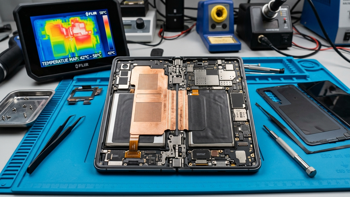
Figure 4: Physical teardown of the thin foldable chassis displaying the copper dual-wing vapor chamber, graphite cooling spreaders, and background FLIR thermal imaging monitor showing heat dissipation constraints (<45°C skin limit).
4.2 Modem Subsystem and Ecosystem Maturity
The Xring O3 compute die concentrates on general-purpose compute, graphics, and neural acceleration. For 5G cellular connectivity and radio frequency front-end (RFFE) operations, current implementations interface with a dedicated external modem solution.
Developing a fully integrated, global-ready 5G modem requires multi-year field testing across hundreds of telecom carriers worldwide, complex patent clearance, and extensive weak-signal software tuning. Prioritizing high-performance compute cores and high-bandwidth memory while pairing with proven external RF subsystems represents a disciplined commercial launch strategy.

Figure 5: First-person perspective holding the unfolded foldable device running on-device computer vision object tracking alongside real-time voice translation without cloud latency.
05 Global Semiconductor Implications: China’s Evolution from System Integrator to Silicon Architect
The debut of the Xiaomi Xring O3 carries ramifications that extend well beyond a single generation of foldables or tablets.
5.1 Beyond Off-the-Shelf Reference Designs
Android OEMs previously relied on uniform configurations combining standard ARM CPU/GPU designs with standard memory interfaces, competing primarily on thermal dissipation surface area and clock frequency tuning. The Xring O3 demonstrates that top-tier OEMs can define custom silicon architectures from the ground up—customizing standard cell libraries, rebalancing core topologies, and co-designing memory controllers to serve proprietary OS requirements (Xiaomi HyperOS) and edge neural models (MiMo).
5.2 Enabling High-Throughput Edge AI
With 200 TOPS INT4 tensor throughput and 113.8 GB/s memory bandwidth, multi-billion parameter multimodal models can execute locally without cloud round-trip latencies or privacy compromises. Real-time multilingual voice translation, visual scene reasoning, and cross-device agentic interactions execute directly on-chip within the Xiaomi 18 Fold and Pad 9 Pro Max.
5.3 Parallel Evolution Across Frontier Sectors
Across FYZSXNB’s research series, a broader technological transition is apparent:
- From BYD’s Blade Battery 2.0 and FLASH charging architecture redefining global EV charging infrastructure;
- To in-house automotive compute platforms (NIO Shenji NX9031, XPENG Turing, and BYD Xuanji A3) establishing proprietary intelligent vehicle computing layers;
- To Xiaomi entering top-tier flagship mobile SoC engineering with the Xring O3.
China’s technology leaders are systematically evolving from hardware assemblers into architects of foundational compute, energy, and AI infrastructure. The Xring O3 signals that the prerogative to define next-generation computing silicon belongs increasingly to innovators operating at the intersection of large-scale commercial deployments and vertically integrated software ecosystems.

Figure 6: Twilight editorial photography outside an illuminated technology campus, highlighting the unified ecosystem connecting high-performance electric vehicles, smart cockpits, and flagship mobile devices.