—
01 Why Are Chinese Automakers Developing In-House Silicon?
In the traditional automotive industry, the division of labor between automakers (OEMs) and semiconductor vendors was strictly partitioned: OEMs engineered vehicles and chassis dynamics; Tier 1 suppliers assembled integrated electronic control modules; and the foundational digital compute silicon was provided by specialized semiconductor giants such as NXP, Infineon, NVIDIA, and Qualcomm.
Between 2024 and 2026, however, this established global division of labor underwent a profound shift in China’s intelligent electric vehicle (EV) sector.
From NIO deploying its in-house 5nm automotive-grade AI SoC, the Shenji NX9031, on its flagship ET9 luxury sedan , to XPENG unveiling its Turing AI Chip for applications across electric vehicles, robotics, and flying vehicles , and BYD scaling mass production of its 4nm Xuanji A3, which delivers over 2100 TOPS across a three-chip coordinated cluster —leading Chinese automakers have progressively cleared the formidable engineering hurdles of custom silicon design.
The driving force behind this transition is evident: the iterative pace of software models and assisted driving algorithms is advancing substantially faster than traditional automotive hardware refresh cycles. As intelligent-driving and advanced driver-assistance stacks are evolving rapidly from rule-based architectures and standard convolutional neural networks (CNNs) to end-to-end foundation models, Vision-Language-Action (VLA) networks, and world models, general-purpose commercial chips—with their architectural compromises in memory bandwidth, sensor ingestion latency, and energy efficiency—can no longer fully satisfy automakers seeking peak efficiency for their proprietary neural network pipelines.
—
Conceptual illustration of automotive AI silicon and software convergence. FYZSXNB Editorial Graphic (Tier V4). Conceptual visualization – not a real-world vehicle blueprint.
02 Why Did the Industry Initially Standardize on NVIDIA Orin?
Between 2021 and 2024, NVIDIA’s DRIVE Orin-X platform became an important industry compute benchmark across high-end intelligent vehicles .
Fabricated on a 7nm process with 17 billion transistors, a single Orin-X SoC integrates a 12-core ARM CPU and an Ampere-architecture GPU, delivering up to 254 INT8 TOPS of nominal compute . Leading EV manufacturers widely adopted dual Orin-X (508 TOPS) or quad Orin-X (1016 TOPS) configurations.
Automakers standardized on Orin for three core reasons:
• Robust General-Purpose Parallel Compute: The Ampere GPU architecture offered exceptional programming flexibility, accommodating rapidly shifting perception algorithms;
• Mature CUDA Ecosystem: Models trained in the cloud could be seamlessly deployed onto vehicles via TensorRT with minimal translation overhead;
• De-risking Early Innovation: Procuring a proven commercial platform allowed automakers to bypass massive upfront silicon R&D expenditures while algorithmic paradigms were still fluid.
However, as algorithms evolved toward end-to-end Transformers and as production vehicle volumes expanded, the structural trade-offs of general-purpose platforms emerged:
• Bill-of-Materials (BOM) Costs: Multi-chip configurations added substantial hardware cost per vehicle;
• Silicon Redundancy and Memory Bottlenecks: General-purpose GPU shaders contain architectural overhead not utilized by Transformer inference, limiting real-world efficiency;
• Sensor Ingestion Bottlenecks: As camera resolution and sensor data volumes increased, the latency and bandwidth of on-die Image Signal Processors (ISPs) became critical; simultaneously, continuous high-throughput data streams from LiDARs and radars over high-speed interfaces imposed severe demands on memory bus bandwidth and task schedulers.
These factors compelled full-stack software-capable automakers with substantial delivery volumes to explore custom silicon tailored specifically to their algorithm pipelines.
—
03 NIO Shenji NX9031: Full-Stack Integration and Foundational Silicon
NIO’s flagship silicon milestone is the Shenji NX9031, announced in late 2023 .
┌────────────────────────────────────────────────────────────────────────────────────────┐
│                   VERIFIED SPEC SNAPSHOT: NIO SHENJI NX9031                            │
├────────────────────────────────────────────────────────────────────────────────────────┤
│   • Process & Density: 5nm Automotive Grade / >50 Billion Transistors                  │
│   • CPU Topology: 32-Core Heterogeneous Big/Little / ASIL-D Functional Safety          │
│   • Official Performance Metric: "Equivalent to 4 Flagship Chips"                      │
│     (Absolute TOPS metric not publicly disclosed)                                      │
│   • Vision Pipeline: 6.5 GPixel/s ISP Throughput / ISP Processing Latency <5ms         │
│   • Memory Subsystem: 546 GB/s LPDDR5x High-Speed Interface                            │
│   • System Integration: Deeply optimized with SkyOS for the ET9 Flagship Sedan         │
└────────────────────────────────────────────────────────────────────────────────────────┘
3.1 Hardware Architecture and Official Metrics
According to NIO official disclosures, the Shenji NX9031 is fabricated on a 5nm automotive-grade process, packing over 50 billion transistors onto a single chip, integrated with a 32-core heterogeneous CPU and a 546 GB/s memory bus .
Regarding compute performance, NIO’s official baseline statement is: “A single Shenji NX9031 delivers performance equivalent to four current industry flagship chips” .
*【Technical Audit Note: NIO has not published a discrete numerical TOPS figure directly comparable to standard spec sheets; the baseline reference remains its official equivalence statement. Consequently, this analysis does not convert the NX9031 into speculative TOPS figures, but evaluates its verified memory bandwidth and image processing pipeline.】*
3.2 Vision Processing Pipeline and System Synergy
Key pipeline highlights of the NX9031 include:
• 6.5 GPixel/s ISP Throughput: Capable of processing multiple concurrent high-definition video streams in real time;
• ISP Image-Processing Latency Under 5ms: Reducing ISP image-processing latency in the visual pipeline;
• Deep Synergy with SkyOS: Serving as the computational anchor for NIO’s whole-vehicle operating system, enabling unified micro-scheduling across drive and spatial perception models.
On the flagship ET9 sedan, the NIO ADAM supercomputing platform comprises two Shenji NX9031 SoCs, one Qualcomm Snapdragon 8295P cockpit chip, and an N-Box subsystem operating in close coordination.
—
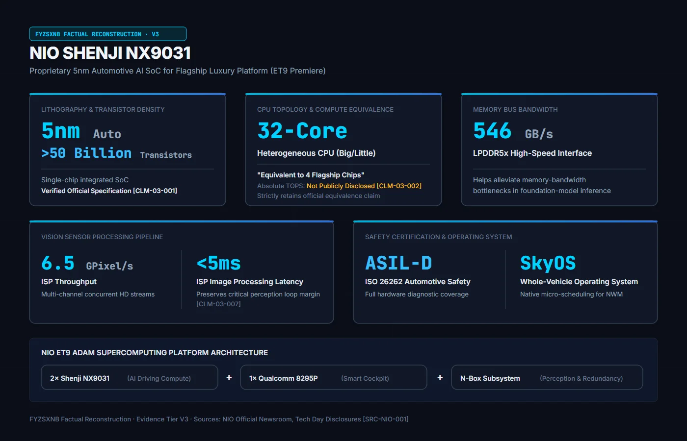
Figure 1: NIO Shenji NX9031 verified hardware specifications and ET9 ADAM platform integration. (Source: NIO Disclosures [SRC-NIO-001])
04 XPENG Turing AI Chip: Dedicated DSA and On-Device Foundation Models
XPENG’s Turing AI Chip is engineered specifically for direct hardware acceleration of end-to-end foundation models across multiple embodied AI form factors .
┌────────────────────────────────────────────────────────────────────────────────────────┐
│                   VERIFIED SPEC SNAPSHOT: XPENG TURING AI CHIP                         │
├────────────────────────────────────────────────────────────────────────────────────────┤
│   • Compute Engine: 40-Core Custom AI Processor / 2× In-House DSA NPUs                 │
│   • Model Capacity: Engineered to run up to 30-Billion Parameter Models on-device      │
│   • Official Performance: 750 TOPS Effective Computing Power (Precision Undisclosed)   │
│   • Vision & Safety: Dual Independent ISPs / ASIL-B (Independent Safety Island ASIL-D) │
│   • Deployment Scope: AI Vehicles, Humanoid Robots (IRON), eVTOL Flying Cars           │
└────────────────────────────────────────────────────────────────────────────────────────┘
4.1 40-Core Custom AI Processor and 30B Model Deployment
Disclosed during XPENG AI Day in November 2024, key architectural features include:
• 40-Core Custom AI Processor: Featuring 2 proprietary Neural Processing Units (NPUs) built on a Domain-Specific Architecture (DSA) optimized for neural network operators;
• On-Device Execution of 30B Parameter Models: Tailored memory allocation and matrix units engineered for local large-model inference without cloud round-trips [CLAIM: CLM-03-003] [SOURCE: SRC-XPENG-001];
• Dual Independent ISPs: Delivering image enhancement for adverse weather, low-light and backlit conditions;
• Functional Safety Certification: The SoC has completed ISO 26262 ASIL-B chip-level certification, with an independent safety island engineered to ASIL-D standards.
4.2 Performance Metrics and Cross-Domain Architecture
XPENG officially states that the Turing chip achieves 750 TOPS of Effective Computing Power, asserting that one chip can replace three high-performance commercial SoCs .
*【Technical Audit Note: XPENG has not disclosed the mathematical precision (e.g. INT8 vs INT4) underlying the 750 TOPS metric. In engineering evaluations, this metric is documented as “750 TOPS Effective Compute (Precision Undisclosed)”.】*
XPENG plans to deploy the Turing chip across AI vehicles, bipedal humanoid robots (IRON), and eVTOL flying cars. *【FYZSXNB Editorial Analysis: Deploying a common compute architecture across automotive, robotics, and aviation domains could broaden the amortization base if sufficient cross-domain production scale is achieved.】*
—
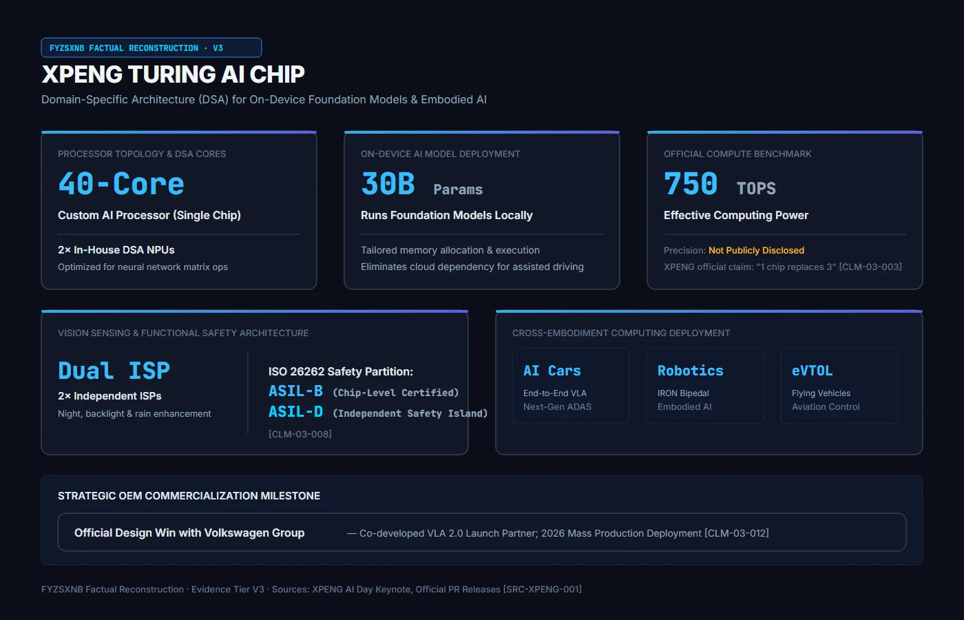
Figure 2: XPENG Turing AI Chip architecture and cross-embodiment computing deployment across cars, robotics, and aviation. (Source: XPENG [SRC-XPENG-001])
05 BYD Xuanji A3: Vertical Integration and Platform Synergy
BYD’s approach to custom silicon reflects deep vertical integration with vehicle manufacturing, positioning its in-house compute as part of the broader whole-vehicle intelligent architecture .
┌────────────────────────────────────────────────────────────────────────────────────────┐
│                   VERIFIED SPEC SNAPSHOT: BYD XUANJI A3 & PLATFORM                     │
├────────────────────────────────────────────────────────────────────────────────────────┤
│   • Fabrication Process: 4nm Automotive Grade / In Active Mass Production              │
│   • System Architecture: Three-Chip Coordinated Cluster / >2100 TOPS Total Compute     │
│   • Efficiency Claims: -20% Power per Compute, +100% Compute Utilization (BYD claims)  │
│   • Core Function: Computing backbone for the God's Eye Intelligent Driving Suite      │
└────────────────────────────────────────────────────────────────────────────────────────┘
5.1 4nm Process and Three-Chip Coordinated Cluster
Fabricated on a 4nm automotive-grade process, the Xuanji A3 is already in active mass production . BYD implements a three-chip coordinated cluster, delivering aggregate system compute exceeding 2100 TOPS .
In official presentations, BYD states that compared to alternative solutions, its in-house chip achieves a “20% reduction in power consumption per unit of compute and a 100% increase in compute utilization efficiency.”
*【Technical Audit Note: These efficiency figures represent manufacturer launch claims; in the absence of standardized third-party benchmarks, they are documented explicitly as “according to BYD”.】*
5.2 System Positioning Within Xuanji Architecture
System engineering requires distinguishing between on-die chip capabilities and whole-vehicle architectural coordination:
• A3 Silicon Role: The A3 provides foundational compute for BYD’s “God’s Eye” driving suite and advanced intelligent-driving capabilities;
• Whole-Vehicle Cross-Domain Synergy: BYD’s distinctive capability lies in Xuanji Architecture 2.0, which orchestrates road-preview perception with the DiSus active body control system and coordinates with the e4 four-motor independent drive platform. This real-time coordination is the product of whole-vehicle electronic and chassis integration, rather than an isolated function of the A3 silicon die alone.
—
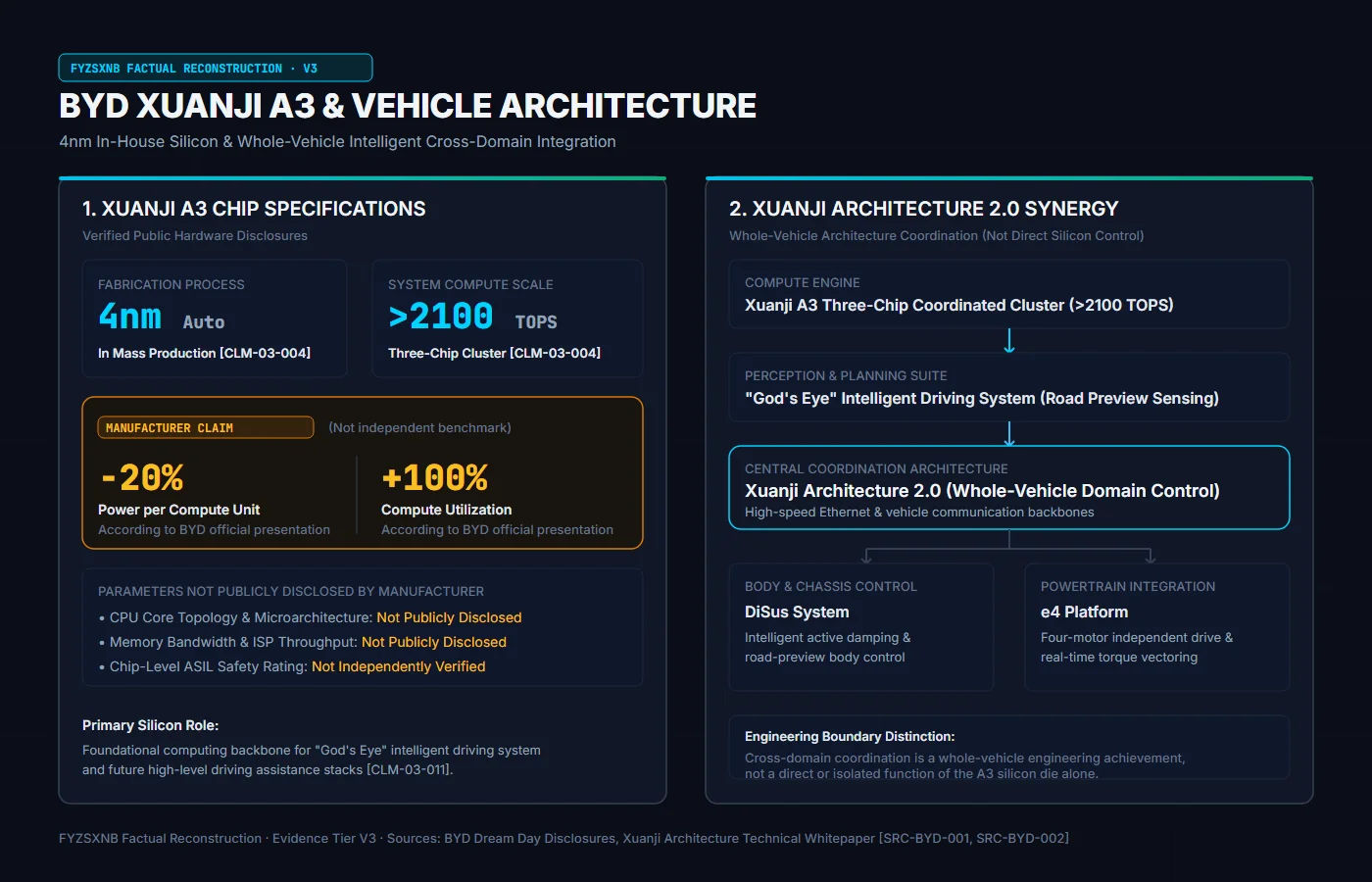
Figure 3: BYD Xuanji A3 silicon specifications and Xuanji Architecture 2.0 whole-vehicle cross-domain integration. (Source: BYD Disclosures [SRC-BYD-001])
06 Evaluating Compute Metrics: Why TOPS Alone Does Not Define Performance
In automotive marketing, processor performance is frequently simplified into a single metric: TOPS (Trillions of Operations Per Second). In semiconductor and automotive engineering, however, direct comparison of TOPS numbers across disparate architectures and testing baselines is fundamentally incomplete.
┌────────────────────────────────────────────────────────────────────────────────────────┐
│                   UNDERSTANDING COMPUTE METRICS BEYOND RAW TOPS                        │
├────────────────────────────────────────────────────────────────────────────────────────┤
│   • Precision Discrepancies: INT8, INT4, and FP formats have vastly different density; │
│     lower precision boosts theoretical peak, but requires quantization engineering     │
│   • Sparsity vs Dense Compute: Structured sparsity can increase peak reported          │
│     throughput depending on the metric definition; real gain depends on model structure│
│   • Single Chip vs Multi-Chip: On-die bus latency vs inter-chip interconnect overhead  │
│   • The Memory Wall: Without matching memory bandwidth, compute cores sit idle         │
└────────────────────────────────────────────────────────────────────────────────────────┘
Key engineering dimensions:
• Mathematical Precision: INT8 and INT4 formats differ substantially in computational density. Lower bit-width increases theoretical TOPS, but depends on hardware quantization support and must not compromise perception fidelity;
• Sparsity vs Dense Compute: Some ratings cite peak TOPS with structured sparsity enabled; real-world throughput depends on whether an automaker’s model structure matches that sparsity pattern;
• Single Chip vs Multi-Chip Cluster: Single-chip solutions offer minimal on-chip interconnect latency, while multi-chip clusters scale total capacity via inter-chip buses, involving distinct engineering trade-offs;
• Actual Utilization Efficiency: Real-world performance depends heavily on whether Domain-Specific Architecture (DSA) units match the attention mechanisms of modern Vision Transformers.
Consequently, simple numerical comparisons between 254, 750, and 2100+ TOPS do not directly correlate with real-world driving assistance capability.
—
07 Key Engineering Metrics That Determine Driving Intelligence
In actual vehicular deployment, the key hardware pillars governing compute platforms include:
┌────────────────────────────────────────────────────────────────────────────────────────┐
│                   CRITICAL SYSTEM METRICS IN AUTOMOTIVE COMPUTE                        │
├────────────────────────────────────────────────────────────────────────────────────────┤
│   1. Memory Bandwidth: 546 GB/s on NX9031 helps alleviate memory bottlenecks           │
│   2. On-Die ISP Latency: High throughput and <5ms latency accelerate perception loops  │
│   3. Dedicated DSA Blocks: Can improve efficiency for matched neural-network workloads │
│   4. Thermal & Power Design: Advanced nodes may improve performance-per-watt           │
│   5. Functional Safety / ISO 26262: Diagnostic coverage mitigates fault risks          │
│   6. In-House Compilers & Drivers: Greater stack control streamlines model deployment  │
└────────────────────────────────────────────────────────────────────────────────────────┘
• Memory Bandwidth: End-to-end models require continuous weight and feature map movement from DRAM. The NX9031’s 546 GB/s memory bus [CLAIM: CLM-03-001] [SOURCE: SRC-NIO-001] is engineered to help alleviate memory-bandwidth bottlenecks and minimize core idle time;
• ISP Processing Latency: Integrating high-throughput ISPs (such as 6.5 GPixel/s) on-die keeps image processing latency below 5ms, preserving critical response time for perception and planning;
• Dedicated Transformer Acceleration (DSA): Tailored hardware blocks for attention mechanisms can improve efficiency for matched neural-network workloads compared to generalized compute units;
• Automotive Thermal and Power Design: Under comparable architectures and workloads, advanced process nodes (5nm / 4nm) may improve performance-per-watt, though overall thermal design depends on transistor count, clock frequencies, and vehicle cooling;
• Functional Safety / ISO 26262: Higher ASIL requirements demand stronger hardware safety mechanisms and diagnostic coverage to mitigate fault risks, though specific chip-level certifications differ by platform (e.g. ASIL-D for NX9031, ASIL-B for Turing chip with ASIL-D safety island).
—
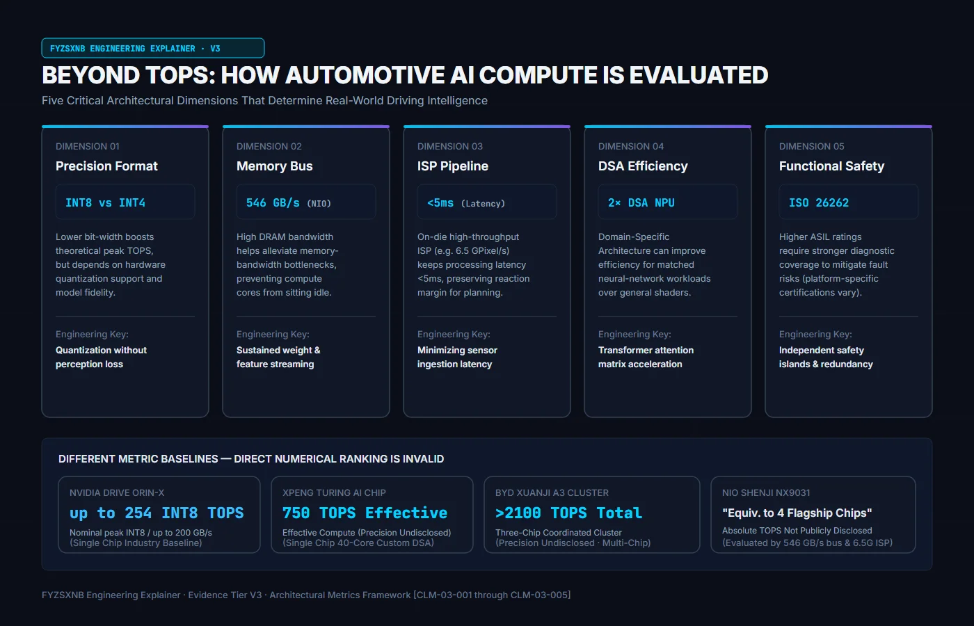
Figure 4: Multidimensional evaluation framework for automotive AI compute beyond raw TOPS marketing metrics. (FYZSXNB Engineering Explainer)
08 Three Automakers, Three Strategic Pathways
A comparative analysis of NIO, XPENG, and BYD illustrates distinct engineering philosophies:
Table 1: Core Hardware Specifications & Official Metrics
| Platform / SoC | Designer | Process Node | Core Topology / CPU | Official Compute Metric | Metric Baseline | Die / System | Public AI / Model Integration Info | ISP Throughput | Memory Bandwidth | Functional Safety | Production Status | Sources & Rating |
|---|---|---|---|---|---|---|---|---|---|---|---|---|
| Shenji NX9031 | NIO | 5nm Auto | 32-Core (Big/Little) | “Equivalent to 4 flagship chips” | Equivalence baseline (No absolute TOPS published) | Single Chip | Runs NIO World Model (NWM) on ET9 platform | 6.5 GPixel/s | 546 GB/s (LPDDR5x) | ASIL-D | Mass production (ET9 premiere) | Grade A / B |
| Turing | XPENG | Undisclosed (Advanced Auto) | 40-Core Custom AI Processor | 750 TOPS Effective Compute (XPENG: “1 replaces 3”) | Precision Undisclosed | Single Chip (Scalable 3-chip 2250 TOPS) | Engineered for up to 30B parameter on-device models | Dual Independent ISPs | Not publicly disclosed | Chip ASIL-B certified; Safety island ASIL-D | Mass produced & powered on | Grade A / B |
| Xuanji A3 | BYD | 4nm Auto | Not publicly disclosed | Three-Chip Cluster >2100 TOPS | Precision Undisclosed (BYD: +100% utilization) | Three-Chip Cluster | Powers BYD AD stack; max model size undisclosed | Not publicly disclosed | Not publicly disclosed | Not independently verified from public BYD sources | In mass production | Grade A |
| DRIVE Orin-X | NVIDIA | 7nm (TSMC) | 12-Core (ARM Cortex-A78AE) | up to 254 INT8 TOPS | INT8 Nominal | Single Chip (Common Dual/Quad setups) | Broad industry support for CNN & Transformer models | 1.85 GPixel/s | up to 200 GB/s (LPDDR5) | ASIL-D | Industry benchmark in mass production | Grade A |
*Note: “Not publicly disclosed” denotes specifications withheld from official public materials; unverified speculative estimates are strictly excluded.*
—
Table 2: FYZSXNB Editorial Analysis — Strategic Differences
| Dimension | NIO | XPENG | BYD |
|---|---|---|---|
| Primary Design Motivation | Safety control, SkyOS operating system synergy, high-speed vision processing | Dedicated DSA for end-to-end models; unified compute across cars, robotics, and aviation | Scaling intelligent driving to mass markets; deep integration with chassis dynamics |
| Algorithm Focus | End-to-end vision + NIO World Model (NWM) spatial forecasting | End-to-end foundation models + embodied AI | Xuanji cross-domain: vision, powertrain, and chassis integration |
| Role in Vehicle Platform | Core compute engine for central vehicle supercomputer | Universal AI processor across diverse embodied platforms | Dedicated intelligent driving compute platform |
| Depth of System Synergy | Silicon ➔ SkyOS ➔ Chassis/Cockpit domains | Silicon ➔ Canghai Platform ➔ Multimodal agents | Silicon ➔ Xuanji Architecture ➔ Coordination with vehicle subsystems |
| Key Competitive Advantage | 6.5 GPixel/s ISP, low latency, massive headroom for luxury flagship | Tailored Transformer acceleration, 30B parameter models on-device | Large vehicle manufacturing scale may provide a broader base for amortizing R&D costs |
| Primary Engineering Challenge | High upfront chip investment must be absorbed over the lifecycle of mid-to-high-end vehicle programs | Maintaining compiler toolchains across heterogeneous form factors | Managing software compatibility across an exceptionally broad vehicle portfolio |
*Note: This table reflects FYZSXNB editorial analysis based on public technical materials and does not represent official manufacturer claims.*
—
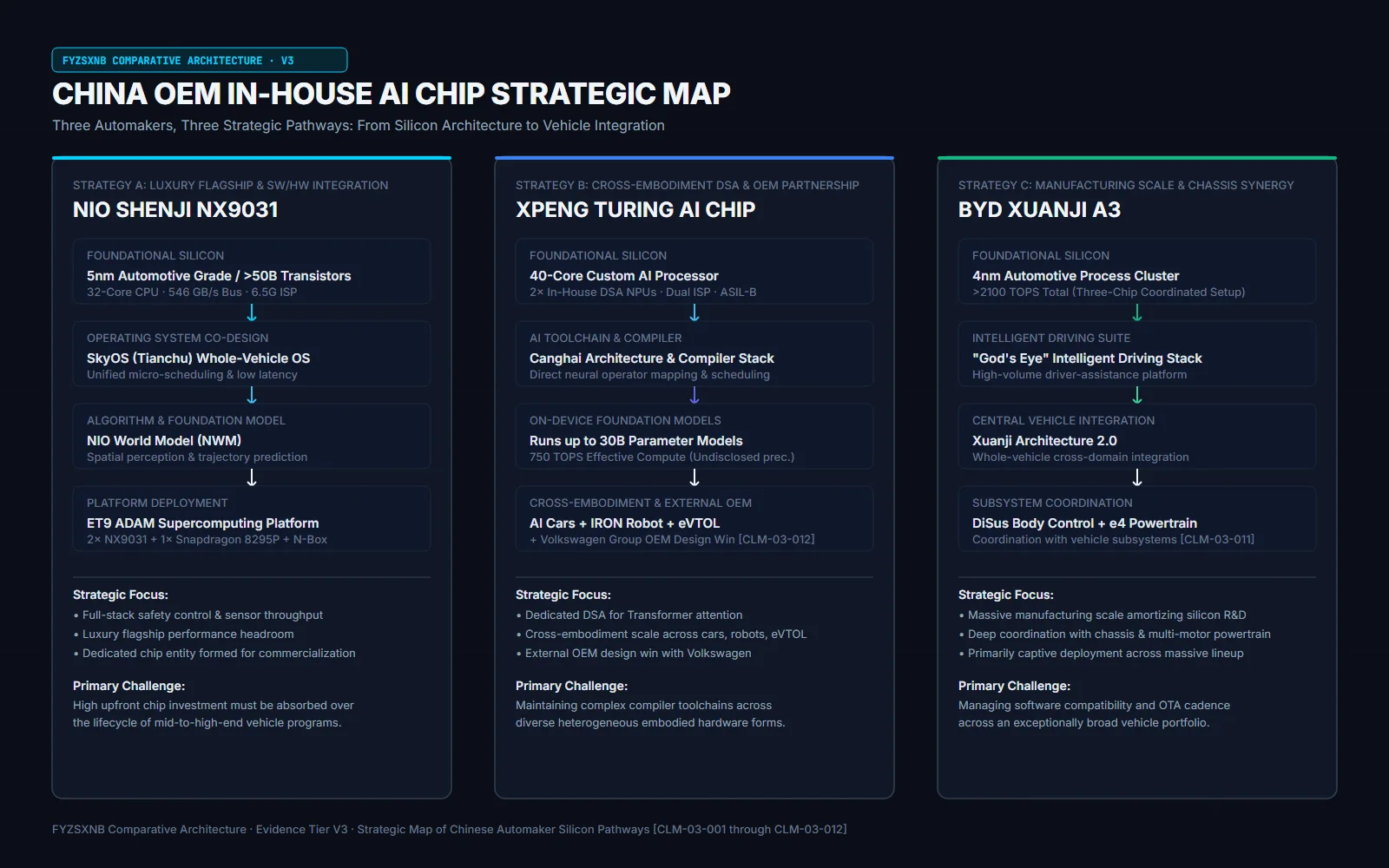
Figure 5: Comparative strategic paradigms of in-house automotive silicon development across NIO, XPENG, and BYD. (FYZSXNB Comparative Analysis)
09 Commercial Drivers: Why Automakers Invest in In-House Silicon
Developing automotive SoCs on advanced nodes requires immense capital expenditures across IP licensing, EDA toolchains, tape-outs, certification, and engineering salaries. Automakers pursue in-house development based on the following strategic calculations:
┌────────────────────────────────────────────────────────────────────────────────────────┐
│                   FINANCIAL & STRATEGIC CONSIDERATIONS IN SELF-DESIGN                  │
├────────────────────────────────────────────────────────────────────────────────────────┤
│   1. Scale Economics: At sufficient volume, custom SoCs may improve cost structure     │
│      and reduce dependence on premium merchant platforms                               │
│   2. Software Autonomy: Greater control over toolchains can streamline neural-operator │
│      deployment                                                                        │
│   3. Supply Chain Resilience: In-house silicon capability may reduce exposure to some  │
│      external supply dependencies                                                      │
└────────────────────────────────────────────────────────────────────────────────────────┘
• Economies of Scale and Cost Structure: At sufficient production volume, yield, and lifecycle support, fixed development costs may be amortized across more vehicles, potentially reducing dependence on premium merchant platforms;
• Control Over Toolchains and Deployment: In-house silicon can give automakers greater control over chip definition, low-level drivers, compiler toolchains, and model deployment. When novel neural network operators emerge, engineering teams can implement targeted optimizations directly without waiting for external vendor SDK updates—though reliance on third-party foundational IP and fabrication foundries persists;
• Supply Chain Resilience: Developing proprietary semiconductor engineering capabilities provides automakers with greater strategic independence during global silicon supply fluctuations.
—
10 Transitioning from System Integration to Hardware-Software Co-Design
In the internal combustion engine era, core automotive competencies centered on engines, transmissions, and mechanical chassis tuning; in the initial phase of electrification, focus shifted to batteries, electric motors, and power electronics.
The deployment of the Shenji NX9031, Turing, and Xuanji A3 marks the arrival of a new era defined by the convergence of custom silicon, vehicle operating systems, and advanced AI algorithms.
This transformation disrupts the traditional “black-box” supply model dominated by global Tier 1 vendors. Automakers are turning vehicles into deeply integrated mobile computing systems, extending their engineering capabilities into semiconductor architecture, vehicle operating systems, and on-device model execution.
—
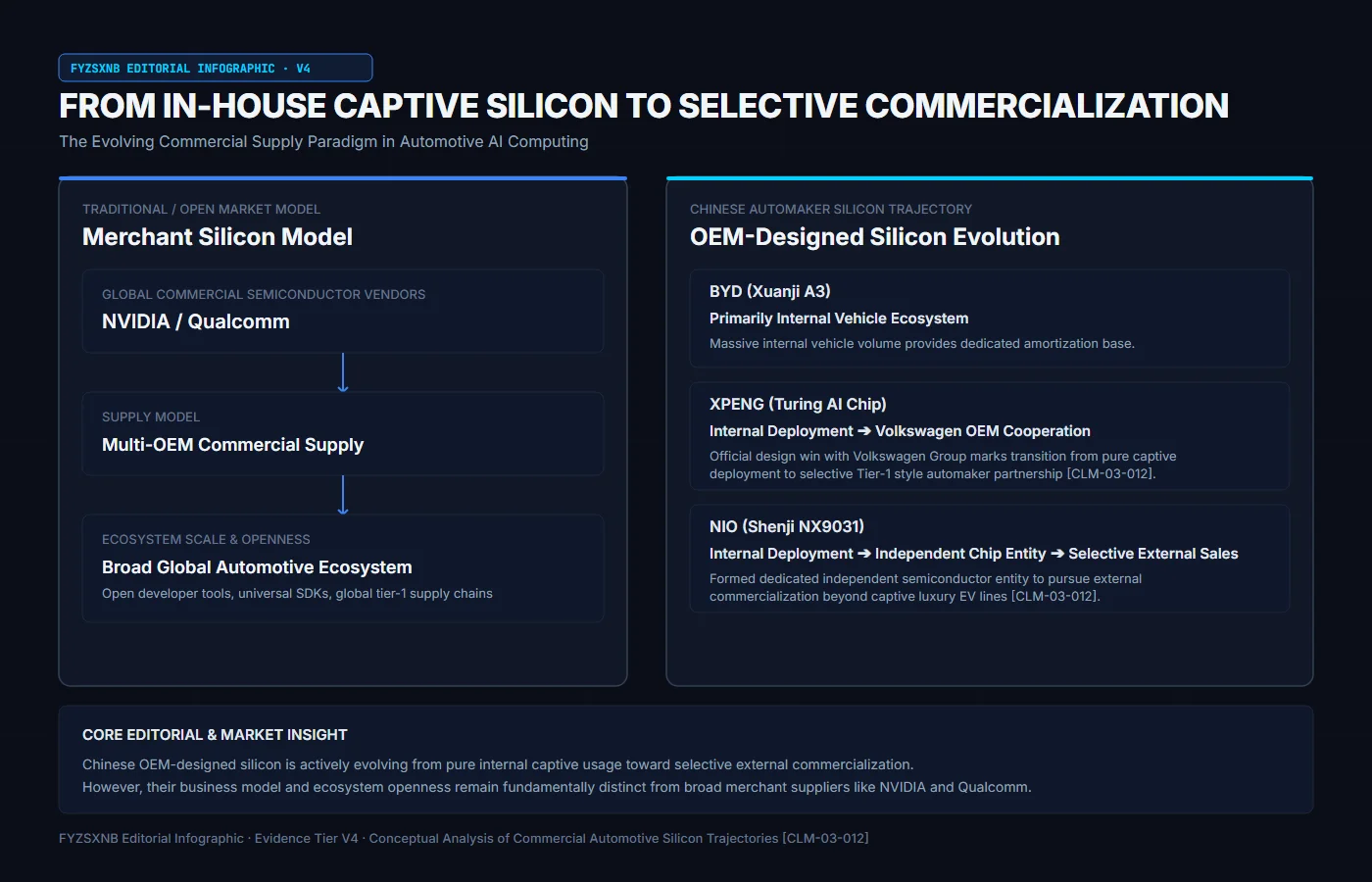
Figure 6: Evolution of automotive AI compute from merchant silicon to selective OEM commercialization. (FYZSXNB Editorial Graphic)
11 Global Market & Regional Implications
For international automotive executives and industry analysts across Europe, Russia, the Middle East, and Southeast Asia, the development of custom silicon by Chinese automakers carries several practical implications:
┌────────────────────────────────────────────────────────────────────────────────────────┐
│                   GLOBAL MARKET & REGIONAL IMPLICATIONS                                │
├────────────────────────────────────────────────────────────────────────────────────────┤
│   1. Software Lifecycle Autonomy: Controlling low-level stacks theoretically extends   │
│      firmware support longevity                                                        │
│   2. On-Device Compute & Compliance: Local model execution facilitates adherence to    │
│      regional data governance frameworks                                               │
│   3. Selective Commercialization: In-house silicon is gradually expanding beyond pure   │
│      internal captive deployment                                                       │
└────────────────────────────────────────────────────────────────────────────────────────┘
*【Industry Analysis & Practical Implications】:*
• Software Lifecycle Autonomy in Export Markets:
Custom silicon provides automakers with autonomy over low-level firmware stacks, reducing exposure to end-of-life cycles from third-party semiconductor vendors. However, real-world Over-the-Air (OTA) update longevity will remain conditioned on an automaker’s regional investment commitments, regulatory homologation, vehicle sales volumes, and initial hardware compute headroom;
• On-Device Compute and Regional Data Regulations:
Regarding cross-border data governance, the EU GDPR does not require all vehicle data to be stored locally within the European Union. Cross-border transfers involving personal data must satisfy applicable lawful-basis and transfer-safeguard requirements, including adequacy decisions or appropriate safeguards where relevant. Russian regulations impose more explicit localization requirements on the collection and database recording/storage of Russian citizens’ personal data. Stronger on-device computing can allow vehicles to perform perception and assisted decision-making without relying on cloud transmission of raw video streams, but whether particular data constitutes personal data and the applicable compliance route depend on the data type and target-market law;
• Distinguishing In-House Silicon from Open Merchant Silicon:
A clear distinction must be maintained between automaker-designed silicon and traditional merchant silicon. The BYD Xuanji A3 currently remains primarily focused on BYD’s own vehicle ecosystem; the XPENG Turing chip has secured an official design win with the Volkswagen Group, transitioning from captive use to external OEM partnership; NIO has organized an independent chip entity to pursue external commercialization. Thus, Chinese OEM silicon is evolving from pure vertical integration toward selective commercialization, though its business model and ecosystem openness remain distinct from broad merchant suppliers like NVIDIA and Qualcomm.
—
12 Conclusion: Entering the Era of Algorithm-Silicon-Vehicle Co-Design
Throughout computing history, major leaps in system efficiency have emerged from the co-design of software algorithms and underlying hardware.
The strategic value of automaker-designed silicon lies in this collaborative engineering paradigm. As NIO integrates the Shenji NX9031 with SkyOS, as XPENG deploys the Turing chip across embodied AI platforms, and as BYD integrates the Xuanji A3 deeply into its broader whole-vehicle intelligent architecture—automotive engineering is advancing from discrete parts assembly to deep, full-stack hardware-software co-design.
The era of algorithm-silicon-vehicle co-design is beginning to take shape.